- English
- French
- German
- Portuguese
- Spanish
- Russian
- Japanese
- Korean
- Arabic
- Greek
- German
- Turkish
- Italian
- Danish
- Romanian
- Indonesian
- Czech
- Afrikaans
- Swedish
- Polish
- Basque
- Catalan
- Esperanto
- Hindi
- Lao
- Albanian
- Amharic
- Armenian
- Azerbaijani
- Belarusian
- Bengali
- Bosnian
- Bulgarian
- Cebuano
- Chichewa
- Corsican
- Croatian
- Dutch
- Estonian
- Filipino
- Finnish
- Frisian
- Galician
- Georgian
- Gujarati
- Haitian
- Hausa
- Hawaiian
- Hebrew
- Hmong
- Hungarian
- Icelandic
- Igbo
- Javanese
- Kannada
- Kazakh
- Khmer
- Kurdish
- Kyrgyz
- Latin
- Latvian
- Lithuanian
- Luxembou..
- Macedonian
- Malagasy
- Malay
- Malayalam
- Maltese
- Maori
- Marathi
- Mongolian
- Burmese
- Nepali
- Norwegian
- Pashto
- Persian
- Punjabi
- Serbian
- Sesotho
- Sinhala
- Slovak
- Slovenian
- Somali
- Samoan
- Scots Gaelic
- Shona
- Sindhi
- Sundanese
- Swahili
- Tajik
- Tamil
- Telugu
- Thai
- Ukrainian
- Urdu
- Uzbek
- Vietnamese
- Welsh
- Xhosa
- Yiddish
- Yoruba
- Zulu
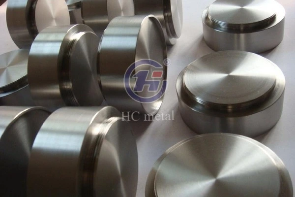
Planar titanium sputtering target
Uniform Density: Ensures stable sputtering rates and consistent thin film quality.
Excellent Thermal Stability: Performs reliably under high sputtering temperatures.
Good Electrical Conductivity: Supports efficient sputtering and coating processes.
Precise Dimensions: Customizable in diameter, length, width, and thickness.
Strong Bonding Options: Compatible with backing plates (Cu, Mo, SS).
Low Impurity Levels: Reduces contamination for high-tech applications.
Wide Compatibility: Suitable for PVD, CVD, and vacuum coating systems.
Consistent Performance: Provides uniform coating thickness and high deposition efficiency.
Application Versatility: Used in optics, electronics, solar, decorative, and semiconductor fields.
Product Introduction
Planar Titanium Sputtering Target for High-Purity Thin Film Deposition — Custom OEM Solutions
Baoji Huacan's planar titanium sputtering target delivers controlled thin-film deposition for semiconductor, display, and hard-coating applications. They are offered in purity levels of 99.5% to 99.995%. Each target has a near-theoretical density (>99.7%), refined equiaxed grain structure less than 50μm, and low oxygen content to avoid micro-arcing. Dimensions, bonding arrangement and surface treatment are totally configurable to suit your system needs.
Product Specification & OEM Customization
|
Parameter
|
Details
|
|---|---|
|
Material
|
High-Purity Titanium (Grade 1, Grade 2, Grade 4)
|
|
Purity Range
|
99.5%–99.995% (2N5–4N5+)
|
|
Grain Size
|
< 50 μm
|
|
Density
|
> 99.7% of Theoretical Density
|
|
Target Shape
|
Circular, Rectangular, or Custom Geometry
|
|
Dimensions
|
Customized to Drawings or Requirements
|
|
Thickness
|
Customized
|
|
Bonding Options
|
Copper (Cu), Molybdenum (Mo), or Stainless Steel (SS) Backing Plate
|
|
Bonding Method
|
Diffusion Bonding or Indium Soldering
|
|
Surface Finish
|
Natural, Polished, or Custom Finish
|
|
Material Standards
|
ASTM B265; SEMI Guidelines
|
Product Application
Semiconductor ICs

01
Flat Panel Displays

02
Hard Coatings
03
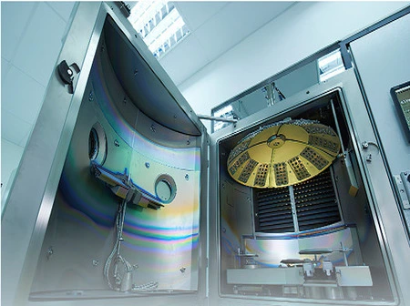
Semiconductor ICs: Titanium is deposited as a wetting layer and TiN diffusion barrier inside contact holes and vias. Purity of 5N+ is required here to prevent aluminum or copper spiking into silicon junctions.
Flat Panel Displays (TFT-LCD & OLED): Large-area rectangular targets deposit low-resistivity gate and source/drain electrodes. High power densities are applied to ensure rapid, uniform deposition across large substrates.
Hard Coatings (Tools & Aerospace): Reactive sputtering with titanium targets produces TiN and TiAlN coatings reaching hardness values up to 3,000 HV. Stable, arc-free sputtering over long production cycles is essential here.
Factory Show
Why Choose Our Planar Titanium Sputtering Target
Your thin film technique requires consistency. Our targets are made from proven high purity titanium billets which are subjected to thermal mechanical processing (TMP) to remove micro-porosity and segregation flaws, the main causes of arcing and nodule development during sputtering.
With over 10 years expertise in titanium machining and 1,000+ tons yearly production capability, we provide both prototype and big volume OEM orders. Every target ships with full material traceability documentation.
 |
 |
 |
Manufacturing Process
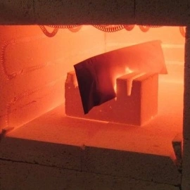
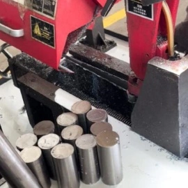
Titanium billets are first refined using vacuum arc remelting (VAR) to achieve chemical homogeneity and low impurity levels. The material then undergoes thermal mechanical processing (TMP), which refines grain structure and establishes a preferred crystallographic texture perpendicular to the target surface — maximizing sputtering yield.
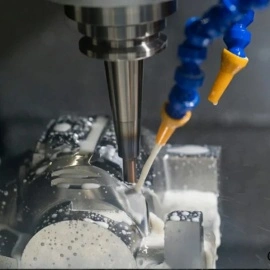
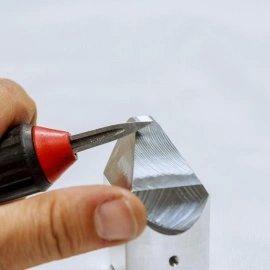
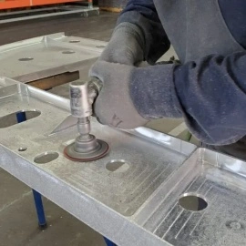
Precision CNC machining follows, using our 40+ advanced machining centers to produce exact geometries per your drawings. Bonding to the backing plate is performed through diffusion bonding for high-power-density applications, or indium soldering for standard use cases.



Manufacturing Capability
We have more than 40 CNC lathes, machining centers and gantry systems. The annual manufacturing capacity reaches 1000 tons. Our partner furnaces for VAR and PAM have a melting capacity of over 5,000 tons/year, allowing us to serve big orders with a dependable supply of raw materials.
 |
 |
 |
 |
 |
| melting | melting | forging | forging | rolling |
Quality Control
Every planar titanium sputtering target batch goes through a structured multi-stage inspection:
· GDMS analysis — detects metallic impurities at parts-per-billion level
· LECO gas analysis — monitors oxygen, nitrogen, and carbon interstitial content
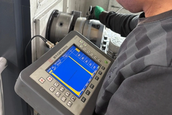
· Ultrasonic C-scan — maps bonding interface integrity
· Metallographic inspection — verifies grain size and phase distribution
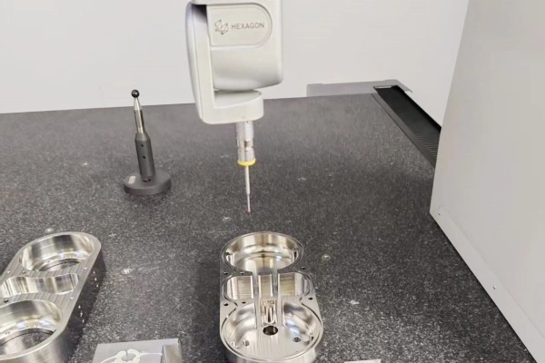
· CMM dimensional inspection — confirms geometry against drawing tolerances
· Surface roughness testing — ensures finish meets deposition process requirements
Full documentation including MTC, inspection reports, and material traceability records ships with every order.
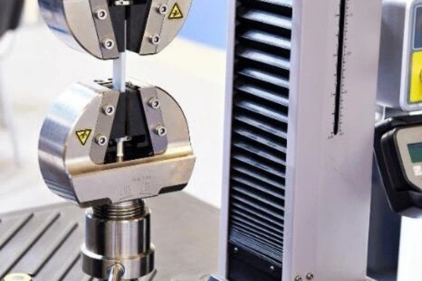
Mechanical Properties Testing
Inner Diameter Measurement

Ultrasonic Testing
CMM Dimensional
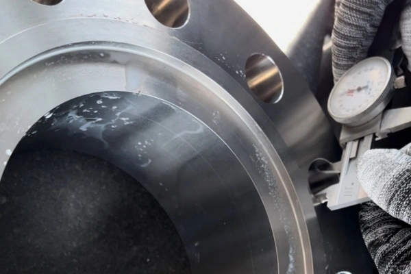
Mounting Hole Diameter Measurement
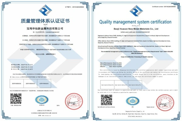
Quality Management System Certification
Packaging & Shipping
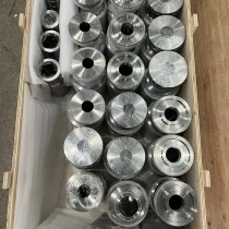
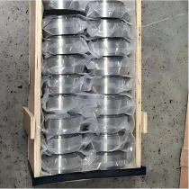
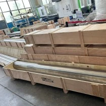
Each target is vacuum packed in bags with desiccants to guard against moisture and packaged in bespoke foam inserts within heavy wooden boxes. Each package includes detailed labeling and paperwork to support tracking.
We provide global air freight (priority shipments) and marine freight (low-cost bulk shipments).


FAQ
Q: What purity grade should I choose for semiconductor applications?
A:Semiconductor logic and memory devices require 5N (99.999%) or higher. Our targets are available up to 99.995%, with GDMS reports to verify trace impurity levels.
Q: How does grain size affect my deposition results?
A:A grain size below 50μm produces a more consistent sputter rate and reduces localized erosion variation, directly improving film thickness uniformity across your wafer.
Q: What bonding method is better — diffusion bonding or indium soldering?
A:If the application has a high power density, then diffusion bonding is advised. This is because it forms a solid-state atomic connection that can endure greater thermal loads without melting or separation.
Q: Are wasted targets recyclable?
A: Yes. Generally 30-40% planar target utilization is achieved thus high pure titanium may be recovered. Professional recycling services may recover and re-melt the material, cutting your material expenses in the long run.
Q: Do you accept custom drawing-based orders?
A:Absolutely. All dimensions, bonding configurations, and purity grades are customizable based on your technical drawings or specifications.
Contact Us
Ready to source a high-performance planar titanium sputtering target? Send your drawing or inquiry to sherry@hc-titanium.com today.

_1769650615648.jpg)

(1)_1769656715190.jpg)


Learn about our latest products and discounts through SMS or email