- English
- French
- German
- Portuguese
- Spanish
- Russian
- Japanese
- Korean
- Arabic
- Greek
- German
- Turkish
- Italian
- Danish
- Romanian
- Indonesian
- Czech
- Afrikaans
- Swedish
- Polish
- Basque
- Catalan
- Esperanto
- Hindi
- Lao
- Albanian
- Amharic
- Armenian
- Azerbaijani
- Belarusian
- Bengali
- Bosnian
- Bulgarian
- Cebuano
- Chichewa
- Corsican
- Croatian
- Dutch
- Estonian
- Filipino
- Finnish
- Frisian
- Galician
- Georgian
- Gujarati
- Haitian
- Hausa
- Hawaiian
- Hebrew
- Hmong
- Hungarian
- Icelandic
- Igbo
- Javanese
- Kannada
- Kazakh
- Khmer
- Kurdish
- Kyrgyz
- Latin
- Latvian
- Lithuanian
- Luxembou..
- Macedonian
- Malagasy
- Malay
- Malayalam
- Maltese
- Maori
- Marathi
- Mongolian
- Burmese
- Nepali
- Norwegian
- Pashto
- Persian
- Punjabi
- Serbian
- Sesotho
- Sinhala
- Slovak
- Slovenian
- Somali
- Samoan
- Scots Gaelic
- Shona
- Sindhi
- Sundanese
- Swahili
- Tajik
- Tamil
- Telugu
- Thai
- Ukrainian
- Urdu
- Uzbek
- Vietnamese
- Welsh
- Xhosa
- Yiddish
- Yoruba
- Zulu
Planar titanium sputter target
Uniform Density: Ensures stable sputtering rates and consistent thin film quality.
Excellent Thermal Stability: Performs reliably under high sputtering temperatures.
Good Electrical Conductivity: Supports efficient sputtering and coating processes.
Precise Dimensions: Customizable in diameter, length, width, and thickness.
Strong Bonding Options: Compatible with backing plates (Cu, Mo, SS).
Low Impurity Levels: Reduces contamination for high-tech applications.
Wide Compatibility: Suitable for PVD, CVD, and vacuum coating systems.
Consistent Performance: Provides uniform coating thickness and high deposition efficiency.
Application Versatility: Used in optics, electronics, solar, decorative, and semiconductor fields.
Product Introduction
Planar Titanium Sputter Target for PVD Coating — High Purity, Custom Dimensions & Stable Deposition Performance
Baoji Huacan's planar titanium sputter target delivers purity grades from 99.5% to 99.995%, with grain size averaging below 20µm and density exceeding 99.7% (≈4.50 g/cm³). Engineered for magnetron sputtering and PVD systems, it ensures uniform deposition, minimal arcing, and low contamination across semiconductor, solar, and display applications. Dimensions, thickness, and bonding configurations are fully customizable to your system requirements. Whether you're sourcing for R&D or volume production, our targets are manufactured under ISO 9001-certified processes with full material traceability.
Product Features

· High Purity: 99.5% to 99.995% grades reduce film resistivity and prevent device failure in sensitive nodes
· Fine Grain Structure: <20µm average grain size ensures uniform sputter yield and consistent film thickness
· High Density: ≥99.7% density minimizes virtual leaks and nodule formation
· Low Oxygen Content: Reduces target poisoning and arcing during reactive sputtering
· Excellent Thermal Stability: Performs reliably under sustained high-power sputtering loads
· Backing Plate Compatibility: Cu, Mo, and stainless steel options for optimized heat dissipation
|
Parameter
|
Details
|
|---|---|
|
Material Grade
|
Titanium Grade 1, Grade 2, Grade 5, Grade 7, and more
|
|
Purity
|
99.5%–99.995%, depending on material grade and requirements
|
|
Density
|
Up to ≥99.7% of theoretical density (approx. 4.50 g/cm³), where applicable
|
|
Grain Size
|
Average grain size: less than 20 μm, subject to specifications
|
|
Oxygen Content
|
Customizable; below 100 ppm for applicable high-purity specifications
|
|
Dimensions
|
Custom sizes available for diameter, length, width, and thickness
|
|
Shape
|
Circular or rectangular
|
|
Backing Plate
|
Copper (Cu), molybdenum (Mo), or stainless steel (SS), optional
|
|
Bonding Method
|
Indium bonding or diffusion bonding
|
|
Surface Finish
|
Natural, polished, or customized
|
|
Material Standards
|
ASTM, AMS, ISO, and DIN, depending on material grade and product specifications
|
Product Application
Solutions One

01
Solutions One

02
Solutions One

03
Solutions One

04
Semiconductor Manufacturing: Ti and TiN barrier layers in DRAM and 3D NAND fabrication. High purity prevents electromigration in sub-10nm contact structures.
Flat Panel Displays (TFT-LCD & OLED): Uniform gate electrode deposition across large-generation glass substrates. Planar geometry minimizes mura defects.
Advanced Photovoltaics (CIGS/Perovskite): Titanium adhesion and back-contact layers that withstand 25-year thermal cycling without delamination.
Optical & Decorative Coatings: Used in PVD and vacuum coating systems requiring consistent thin film uniformity for planar titanium sputter target.
Why Choose Us
Why Choose Our Planar Titanium Sputter Target
Nodule formation, arcing, and uneven film thickness are common headaches in sputtering operations. These issues often trace back to poor target density, large grain structures, or oxygen inclusions in the base material.
Our targets are produced using vacuum arc remelting (VAR) and thermo-mechanical processing. This eliminates porosity, segregation, and dielectric inclusions — three of the most frequent causes of process disruption.
You also get full dimensional flexibility. Diameter, thickness, width, and bonding configuration are all adjustable based on your drawings or system specs.
 |
 |
 |
 |
 |
 |
 |
 |
Manufacturing Process
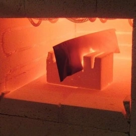
Production begins with high-purity titanium ingots refined through VAR or plasma arc melting (PAM), ensuring chemical homogeneity and ultra-low impurity profiles.
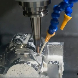
Ingots then undergo precision thermo-mechanical processing to achieve the fine, equiaxed grain structure essential for consistent sputter yield. CNC machining with over 40 precision centers brings each target to its final dimensional specification.
Backing plate bonding — where required — is performed under controlled conditions. Diffusion bonding is recommended for high-power applications (>20 W/cm²) due to its superior shear strength and resistance to thermal expansion mismatch.




Manufacturing Capability
· 40+ CNC lathes and machining centers, including gantry systems
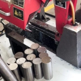
· Annual production capacity exceeding 1,000 tons
· VAR and PAM melting with annual capacity over 5,000 tons
· Forging capacity over 3,000 tons annually
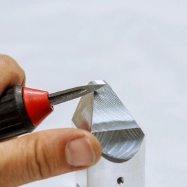
· 10+ years of titanium precision machining experience
· Small batch, prototype, and mass production all supported
 |
 |
 |
 |
 |
| melting | melting | forging | forging | rolling |
Quality Control
BJHC operates a multi-stage inspection protocol specifically relevant to sputter target production:
GDMS Testing: Verifies metallic impurities (Fe, Ni, Cr) down to ppb levels, confirming 4N5 to 5N+ purity.
Inert Gas Fusion (LECO): Measures gaseous impurities — oxygen, nitrogen, carbon — the primary drivers of arcing and target poisoning.
Ultrasonic C-Scan: Maps bonding interface uniformity. Bonding ratio must exceed 98% before shipment approval.
Metallographic Analysis: Confirms grain size (per ASTM E112) and crystallographic texture uniformity.
CMM Dimensional Inspection: Flatness, parallelism, and all critical dimensions verified before final packaging.
Certifications
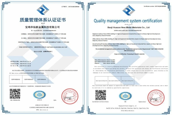
· ISO 9001 Quality Management System Certified
· Material Test Certificates (MTC) available
· EN10204 3.1 documentation available on request
· Full material traceability records provided with every shipment
Mechanical Properties Testing

Inner Diameter Measurement

Ultrasonic Testing

CMM Dimensional
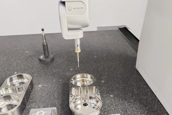
Mounting Hole Diameter Measurement

Quality Management System Certification
Packaging & Shipping
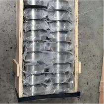
· Vacuum-sealed bags with desiccants for moisture protection
· Custom foam inserts to prevent surface damage during transit
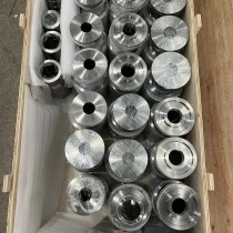
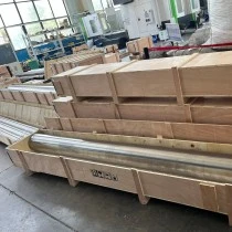
· Sturdy wooden crates for bulk or multi-piece shipments
· Detailed labeling and documentation for customs and traceability
· Air freight (urgent orders) and sea freight (bulk/cost-sensitive) both available


FAQ
Q: Why are nodules forming on my target surface?
A:Nodules typically result from low-density zones or oxide inclusions. Targets with ≥99.7% density and fine grain structure significantly reduce this risk.
Q: How does grain size affect film uniformity?
A:Grain size below 20µm ensures atoms are ejected at a consistent rate and angle. Larger or inconsistent grains cause thickness variation across the substrate.
Q: Which bonding method suits high-power sputtering?
A:Diffusion bonding is recommended above 20 W/cm². It offers higher shear strength and better tolerance for thermal expansion mismatch compared to indium bonding.
Q: What causes arcing during titanium deposition?
A:Arcing is typically triggered by dielectric regions (e.g., titanium oxide from gas impurities) or internal inclusions. Low-oxygen targets with verified LECO testing are the primary solution.
Q: Can you produce targets to match our existing equipment specs?
A:Yes. Send your system drawings or dimensional requirements, and our team will produce a fully matched product to your specification.
Upgrade Your Vehicle's Performance Today
Ready to source a reliable planar titanium sputter target? Contact our team at sherry@hc-titanium.com for a custom quote.
_1755758373045.jpg)



Learn about our latest products and discounts through SMS or email