- English
- French
- German
- Portuguese
- Spanish
- Russian
- Japanese
- Korean
- Arabic
- Greek
- German
- Turkish
- Italian
- Danish
- Romanian
- Indonesian
- Czech
- Afrikaans
- Swedish
- Polish
- Basque
- Catalan
- Esperanto
- Hindi
- Lao
- Albanian
- Amharic
- Armenian
- Azerbaijani
- Belarusian
- Bengali
- Bosnian
- Bulgarian
- Cebuano
- Chichewa
- Corsican
- Croatian
- Dutch
- Estonian
- Filipino
- Finnish
- Frisian
- Galician
- Georgian
- Gujarati
- Haitian
- Hausa
- Hawaiian
- Hebrew
- Hmong
- Hungarian
- Icelandic
- Igbo
- Javanese
- Kannada
- Kazakh
- Khmer
- Kurdish
- Kyrgyz
- Latin
- Latvian
- Lithuanian
- Luxembou..
- Macedonian
- Malagasy
- Malay
- Malayalam
- Maltese
- Maori
- Marathi
- Mongolian
- Burmese
- Nepali
- Norwegian
- Pashto
- Persian
- Punjabi
- Serbian
- Sesotho
- Sinhala
- Slovak
- Slovenian
- Somali
- Samoan
- Scots Gaelic
- Shona
- Sindhi
- Sundanese
- Swahili
- Tajik
- Tamil
- Telugu
- Thai
- Ukrainian
- Urdu
- Uzbek
- Vietnamese
- Welsh
- Xhosa
- Yiddish
- Yoruba
- Zulu
High purity titanium sputtering targets
Uniform Density: Ensures stable sputtering rates and consistent thin film quality.
Excellent Thermal Stability: Performs reliably under high sputtering temperatures.
Good Electrical Conductivity: Supports efficient sputtering and coating processes.
Precise Dimensions: Customizable in diameter, length, width, and thickness.
Strong Bonding Options: Compatible with backing plates (Cu, Mo, SS).
Low Impurity Levels: Reduces contamination for high-tech applications.
Wide Compatibility: Suitable for PVD, CVD, and vacuum coating systems.
Consistent Performance: Provides uniform coating thickness and high deposition efficiency.
Application Versatility: Used in optics, electronics, solar, decorative, and semiconductor fields.
Product Introduction
High Purity Titanium Sputtering Targets — Premium PVD Source Material for Semiconductor & Advanced Coating Applications
Baoji Huacan's high purity titanium sputtering targets are precision-engineered PVD source materials designed for semiconductor, flat panel display, solar, and advanced coating applications. Available in purity grades from 99.5% to 99.995%, these targets deliver uniform density, low oxygen content, and fine grain structure to ensure consistent thin film performance. Whether you need standard dimensions or fully customized geometries, our targets are manufactured to your exact specifications — including diameter, thickness, and backing plate compatibility.
 |
 |
 |
Product Features
| Parameter | Specifications |
|---|---|
| Material | High-Purity Titanium (Ti) |
| Purity | 99.5%–99.995% (2N5–4N5) |
| Density | Approx. 4.506 g/cm³ |
| Grain Size | ≤ 100 μm |
| Oxygen Content | ≤ 500 ppm |
| Dimensions | Custom sizes available: diameter, length, width, and thickness |
| Shape | Round, rectangular, or custom-designed to drawings |
| Backing Plate Materials | Copper (Cu), molybdenum (Mo), or stainless steel (SS) |
| Bonding Options | Diffusion bonding or solder bonding |
| Surface Finish | Machined or polished according to customer requirements |
| Compatible Coating Systems | PVD, magnetron sputtering, and vacuum coating systems |
| Applicable Standards | ASTM, AMS, or other specifications upon request |
| Customization | Purity, dimensions, bonding, and surface finish can be customized to project requirements |

Product Application
Solutions One

01
Solutions One

02
Solutions One

03
Solutions One

04
Semiconductor ICs (Logic & Memory): Titanium films serve as barrier metals and adhesion layers between silicon and metal interconnects. At 7nm and 5nm nodes, target purity directly impacts circuit yield.
Flat Panel Displays (TFT-LCD & OLED): Used for gate and electrode deposition on large-area glass. Uniform grain structure ensures consistent pixel response across 4K and 8K panels.
Photovoltaics & Solar Cells: Titanium coating layers improve contact adhesion and anti-reflection performance in thin-film solar modules.
Optics & Decorative Coatings: Applied in optical interference stacks and decorative PVD coatings requiring precise, repeatable film properties.
Advanced Packaging (TSV): High purity titanium sputtering targets support wetting layer deposition inside high-aspect-ratio through-silicon vias for 3D chip stacking.
Why Choose Us
Our titanium targets are produced from virgin sponge-grade raw material. This eliminates trace contaminants that cause film defects in nanometer-scale processes.
We control grain size to <100μm with uniform equiaxed structure throughout. This prevents uneven erosion patterns and maintains a stable deposition rate across the full target lifetime.
Every target is backed by complete material traceability, dimensional reports, and available GDMS purity certification — giving your procurement and process teams full confidence before the material enters your vacuum chamber |
 |
 |
Manufacturing Process
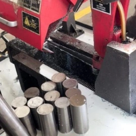
Vacuum arc remelting (VAR) and plasma arc melting (PAM) are used to purify titanium ingots with a high chemical homogeneity and a low level of impurities from the very beginning.
Once melted the material is worked and rolled in a controlled manner to improve the grain structure. The desired equiaxed microstructure and density is obtained by heat treatment.
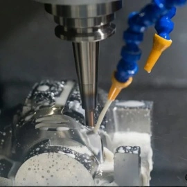
With more than 40 CNC machining centers, we carry out the final shaping, guaranteeing strict dimensional tolerances and fine surface finishes. Each target is then cleaned, examined and vacuum packaged for transportation.






Manufacturing Capability
Our facility in Baoji — China's Titanium Valley — operates with 10+ years of titanium processing experience and an annual production capacity exceeding 1,000 tons.
We maintain 40+ precision CNC machines including machining centers and gantry systems for tight-tolerance target shaping. Our melting and forging capabilities handle ingot production from scratch, giving us full control over material quality from raw sponge to finished target.
 |
 |
 |
 |
 |
| melting | melting | forging | forging | rolling |
Quality Control
Our multi-stage QC process covers every critical inspection point:
· GDMS analysis — verifies trace metallic impurities at ppb level
· LECO analysis — measures gaseous impurities including oxygen, nitrogen, and carbon
· Ultrasonic C-Scan — confirms bonding ratio >98% for bonded target assemblies
· Metallographic inspection — verifies grain size and uniformity via cross-section analysis
· CMM dimensional verification — tolerances within ±0.1mm for tool fitment accuracy
· Surface inspection — roughness measurement and visual defect screening before packaging
Mechanical Properties Testing

Inner Diameter Measurement

Ultrasonic Testing

CMM Dimensional
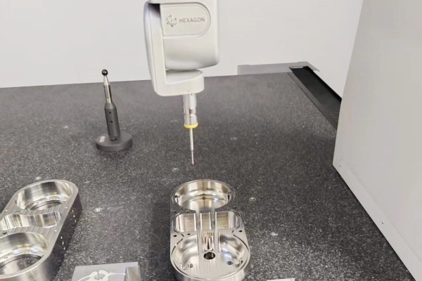
Mounting Hole Diameter Measurement

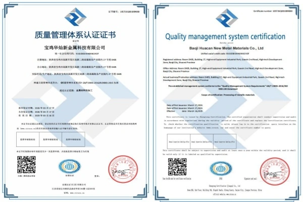
Quality Management System Certification
Packaging & Shipping
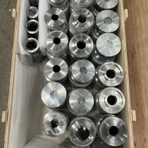
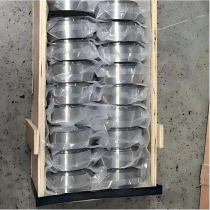
Each target is vacuum-sealed with desiccants to prevent surface oxidation during transit. Custom foam inserts protect the precision-machined surfaces from mechanical damage.
Bulk orders are packed in sturdy wooden crates with full labeling and documentation for easy customs clearance and traceability. Air freight is available for urgent orders; sea freight supports cost-effective bulk shipments.



FAQ
Q: Why does grain size matter for titanium sputtering targets?
A: Fine, uniform grains ensure a constant erosion rate across the target life. Non-uniform grains cause varying deposition rates and nodule formation, which leads to particulate defects in thin films.
Q: What is the difference between diffusion bonding and solder bonding?
A: Solder bonding uses indium and works at lower temperatures. Diffusion bonding forms a solid-state atomic weld, delivering superior thermal transfer — essential for high-power semiconductor processes.
Q: Can you supply product made from recycled material?
A: For semiconductor-grade applications, we use virgin titanium sponge refined via VAR or PAM. This guarantees the trace element control and low alpha-particle emission required by advanced process nodes.
Q: What are your storage requirements for unused targets?
A: Targets are vacuum-packed to prevent oxidation. Shelf life is indefinite if the seal remains intact. Store in a climate-controlled environment to avoid thermal stress on the bond interface.
Q: What documentation can you provide with each order?
A: We provide material test certificates, GDMS purity reports, CMM dimensional reports, and COC documentation. Additional certifications can be arranged based on your requirements.
Contact Us
Ready to source precision titanium targets like high purity titanium sputtering targets? Send your drawings or specifications to sherry@hc-titanium.com and get a fast quote.






Learn about our latest products and discounts through SMS or email